Hardware Acceleration of Image-to-Sketch Style Algorithm Based on Simulink
How to convert image style into sketch ing sotfware and its hardware accelerator based on Simulink
This lecture uses a photo-to-sketch style conversion algorithm to explain:
- How to obtain image patches
- How to use the Pixel Stream Aligner module to align two images with different latencies
- How to use the Line Buffer
- How to reconstruct the control bus
I came across an article on Zhihu titled MATLAB Image Processing: Turning Photos into Sketch Style and thought it would be a great example to demonstrate some techniques of the Vision HDL and HDL Coder toolboxes. Thanks to WYFhiahia for the article.
The photo-to-sketch style conversion algorithm can be roughly divided into the following steps:
- Load the original image as Layer 1 and decolorize it.
- Adjust the curve of Layer 1: output 0, input 40.
- Copy Layer 1 as Layer 2, invert it, and apply a minimum filter.
- Apply color dodge blending.
Step 1: Decolorization
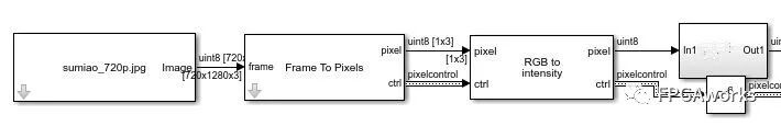
This step converts the color image to grayscale. You can use the Color Space Converter module from the Vision HDL Toolbox or the algorithm we implemented in Lecture 2. For the specific system diagram, refer to the model on GitHub.
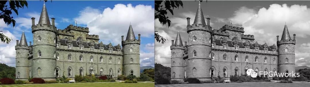
Comparison before and after grayscale conversion:
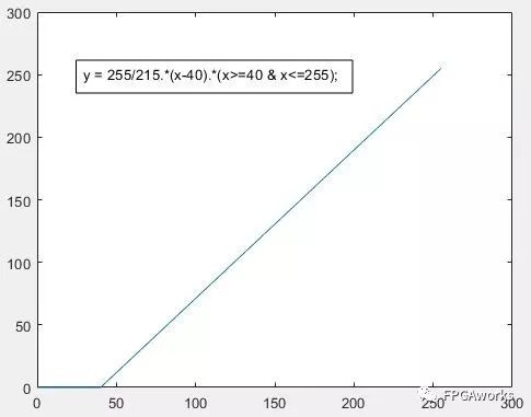
Step 2: Adjust the Curve
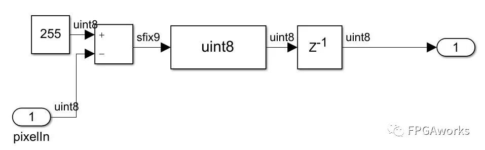
Adjust the curve with output 0 and input 40. This means setting pixel values less than 40 to 0 and mapping the pixel range of 40 - 255 to 0 - 255. Mathematically, this is achieved using a straight line passing through (40, 0) and (255, 255).
The hardware implementation is as follows:
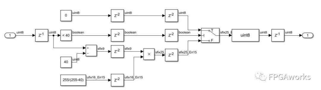
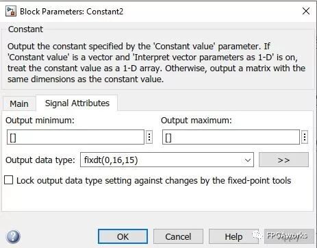
If the input data is less than 40, output 0. Otherwise, subtract 40 and multiply by the constant 255/215. Since 255/215 is not an integer, we can use a Constant module and fix its output format to fixed-point. Here, we use the 0.16.15 format (no sign bit, 1 bit for the integer part, and 15 bits for the fractional part). The setting method is shown in the Output data type below:
During output, all pixels are converted back to the uint8 type. So far, the system is as follows. Since the pixel latency at this step is 6, we set the control bus latency to 6 accordingly.
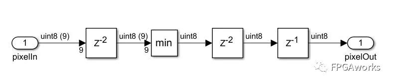
Step 3: Copy, Invert, and Apply Minimum Filter
Copy Layer 1 as Layer 2, invert it, and apply a minimum filter. The inversion module is straightforward: subtract the current pixel value from the maximum value of 255.
Minimum Filter
Theoretically, the minimum filter is used for morphological filtering of binary images. However, here we apply it to grayscale images by taking the minimum value in each 3×3 sliding window as the center pixel value. The patch size can be changed according to the application.
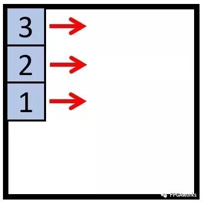
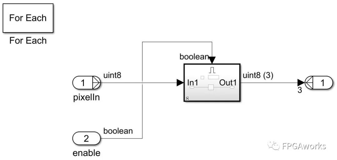
First, we need to extract the 3×3 sliding window. The method is as follows: write the image pixels sequentially into the Line Buffer, which outputs a 3×1 sliding vector. Note that the output is an inverted vector.
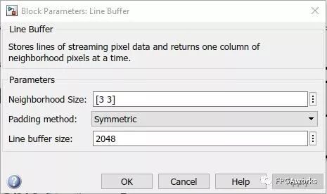
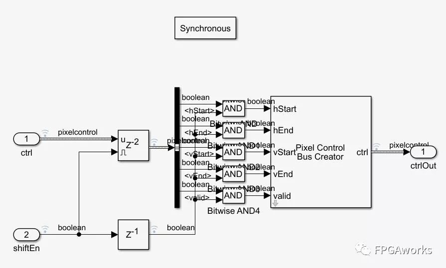
The Line Buffer settings are as follows: for a 3×3 patch, set Neighborhood Size = [3 3]. Set Padding method to Symmetric and Line buffer size to 2048 to meet the storage requirements of 1080p images. Due to padding, the shiftEnable signal will appear one cycle earlier than the valid signal of the control bus.
Next, we need to use a shift register to obtain the 3×3 patch. Here, we use the For Each module. For specific usage, refer to the MATLAB webpage
The specific structure is as follows:
We also need to reconstruct the control bus. Since the output image size is the same as the input, directly delaying the control bus by 2 cycles is acceptable.
Now that we have the 3×3 patch, the next step is to assign the minimum value to the center pixel, as shown below:
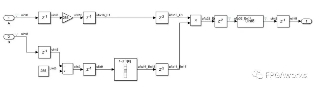
Step 4: Color Dodge Blending
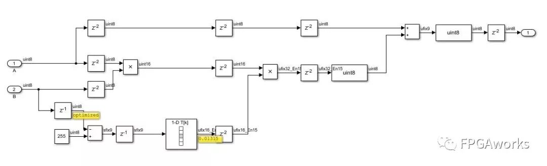
Since the processing times of Layer 1 and Layer 2 are inconsistent, we first need to align these two images using the Pixel Stream Aligner module. refPixel and refCtrl are used to input the later processed image, and the output Pixel and refPixel are then aligned. Then, we perform color dodge blending. I tried three methods:
Method 1 General Color Dodge Blending Algorithm
The algorithm is as follows:
Pixel A + (Pixel A * Pixel B) / Inverted Pixel B
The implementation is as follows. Here, division by inverted Pixel B is achieved through a LookUpTable. Add a Direct Lookup Table (n-D), set it as a 1-D lookup table, and set Table data to [0 1./(1:255)].
The running result is as follows:

Method 2 Formula Provided by the Zhihu Author
1
((uint8)((B == 255) ? B : min(255, ((A << 8 ) / (255 - B)))))
The module implementation is as follows:
The blending result is as follows:
Method 3 Simplest Method: Direct Blending
The result is as follows:
The reason why the first two methods are inconsistent with the original code is that in the minimum filter, I only assigned the minimum value to the center pixel, while the original code assigned it to all pixels in the patch. The results show that direct blending also works well and saves hardware resources.
Hardware Implementation and Optimization
Using the HDL Coder Workflow Advisor, we found that the hardware implementation violated timing requirements. This is because the min module calculates the minimum of 9 inputs. Optimization is needed to meet the timing requirements. The specific method is to divide the 3×3 patch minimum calculation module into column and row parts, each time only calculating the minimum of 3 numbers. Then, re-synthesize to implement the algorithm.
Set the simulation option in the automatically generated Software Interface Model to External and run it. After completion, click Deploy to Hardware. Since images cannot be uploaded now, the final results will be provided on GitHub.
Models, Images, and Final Results
The models, images, and final results are saved in GitHub:
sumiao_zed: For FPGA system generation.sumiao_github: System construction and verification model.sumiao_720p.jpg: Test image.sumiao_result: Comparison of FPGA input and output results.